Arquitectura del Microprocesador 8088
A warning
Each of the Intel x86 series of processors is merely a glorified
calculator chip. I say this in all seriousness. The design lineage
of the x86 line is directly traceable back to the Intel 4004, which
was designed in 1971 as the main chip in a calculator. It was a 4-bit
design. There have been various enhancements since, such as adding
and widening registers, widening internal data paths, widening
external data paths, adding on-board floating point, adding on-board
cache, adding pipelining and superscalar instruction issue, etc., but
at its heart, the x86 is based on a design for a machine with very
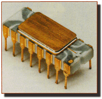
minimal resources. (The picture on the right is a picture of the 4004
chip which I scanned in from BYTE magazine. It was unattributed, but
presumably came from Intel.)
Organization of the 8088
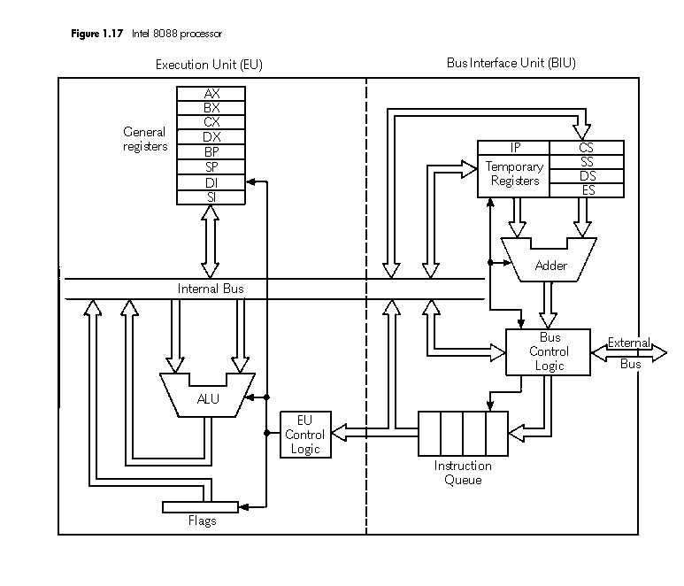
There are two halves to the diagram. On the left is the execution
unit (EU), which is the only part you will generally need to worry
about in writing assembly language programs. On the right is the bus
interface unit (BIU), which you usually won't have to worry about.
The bus interface unit
We'll start with the bus interface unit and describe the function of
each component. The instruction pointer register (IP) holds
the address of the current instruction. You don't have to set this
manually; it gets automatically updated as a part of the fetch-execute
cycle and as the result of branch instructions. Below this are some
temporary registers, which are completely invisible to the
programmer and have to do with instruction decoding and other such
neat stuff. On the right are the four segment registers, which
you can access but generally you leave them alone. These point to
different blocks of memory which have been allocated for your program.
They are used to calculate the absolute memory addresses given offset
addresses given in the program. Below these is an adder, which
is used in this address calculation. The bus control logic
actually handles the electrical communication with memory and various
I/O devices. At the bottom is an instruction queue. The 8088
prefetches instructions in order to reduce the effect of slow memory.
The execution unit
This is the part you get to play with the most. This is the fun part.
At the top of the diagram are the so-called general purpose
registers, which aren't really general-purpose, but as close as
the architecture comes to them. Basically, you can store whatever
values you need in these registers and use them to do computations.
(Of course, you can also make computations on values in memory.) The
reason these are not general purpose registers is that they aren't all
treated the same. Certain instructions expect operands to be in
specific registers. This makes the logistics of register
allocation a little nightmarish. In more modern designs, there is
often a large bank of 32 or more registers (referred to as the
register file), any of which can be used for any operation.
Below this is the internal bus, which is invisible to the programmer
and is used to transfer data within the chip.
Below that is the ALU, or Arithmetic and Logic Unit, which is where
all the actual computations are done (except for the computation of
addresses, noted above).
And then below that is the all-important flags register. The
way the flags register is used is this. Many operations store
information about their results in the flags register. For example,
if the result of a computation was zero, the operation will have as a
side effect setting the zero flag to 1. You can then use a
conditional branch instruction to test that flag and decide
whether or not to branch based on the contents of that flag.
And then, finally, to the right, we see the EU control logic,
which determines, based on the instruction, what signals to send to
the rest of the EU. This is also invisible to the programmer.
